PAGE 9
LOOKING
AT FAULTS
Part 1
|
Maybe you have seen a circuit diagram showing the
signal at various locations.
It does not matter if the waveform is above or below the X-axis. This can be
moved by adjusting the left/right and up/down controls on on the CRO.
When any waveform enters a resistor or capacitor, it emerges
UNCHANGED!
To change any of the characteristics of a waveform, the resistor or capacitor must be connected
to OTHER COMPONENTS.
A square wave will also be attenuated with this circuit:
Two capacitors can also be placed in series to produce an attenuator. This is not
done very often but it has the advantage of providing isolation, such as in this
TOUCH SWITCH circuit.
Now we come to a complex part of the discussion. By placing a resistor and capacitor in series,
different output
waveforms will result.
The two components can be placed in two ways:
If we apply a square-wave to each circuit in Fig 7, the following results are
obtained. (The value of R and C must be selected to achieve these results - but
this will not concern us at the moment.)
The capacitor in Circuit A is pulled up very quickly by the action of the
leading edge of the digital pulse and the value of the capacitor is selected so
that it charges fully during the high-time of the pulse.
This is the amazing part of this circuit.
It is creating a NEGATIVE PULSE!
We are not going into the operation of a differentiator or integrator. They have
been included to show a negative voltage can be produced by a differentiator
circuit.
Inter-stage coupling is also know as "AC coupling" or "Capacitor Coupling."
Capacitor coupling allows each stage to be biased so the DC voltages on one
stage do not affect the next stage. Note: the voltage on the leads of each
coupling capacitor is different.
The 6v p-p waveform generated by the sinewave generator passes thorough the
capacitor and appears at point "X." The DC potential at point "X" is zero
(it is connected to the 0v rail) and
thus the waveform appears equally above and below this level.
You can see the 6v p-p waveform is super-imposed on the DC level (9v) of the
circuit contained within the red dotted rectangle. This is shown in Fig 14.
If you are are fault-finding the circuit and connect a CRO to
different points, quite often you find the waveform is completely different to that on
the circuit diagram.
What do you do?
Is the fault in the circuit?
Is the fault in the CRO?
Or is the picture incorrect?
This is a major dilemma so we have decided to produce this chapter: "Looking
At Faults."
It will guide you through some of the simplest circuits and show you
how components have an effect on a waveform.
The signals flowing through a circuit are very
complex and it is very difficult to show them on a circuit diagram,
due to many factors.
The amplitude will depend on the supply-voltage and this can
decrease as much as 50%, especially in battery-operated equipment.
The other problem is the shape of the waveform. This will depend on the
"quality" of the CRO (the maximum bandwidth) and the setting of the probe (1x or
10x). Your probe may put a load on the circuit and distort the waveform. Or your
CRO may not be fast enough to reproduce the waveform.
If the observer does not see the exact-same waveshape as shown on the circuit, he starts to worry.
I know. I have many overseas circuits showing waveforms and seldom do they correspond to those on the CRO.
This causes enormous frustration.
Is the fault in the section under observation?
Is the fault being introduced by another section?
Or is the fault due to the signal being processed?
We cannot definitively answer any of these and that's why you have to use a CRO with a
lot of understanding.
Because of this, we will limit our discussion to general situations of what to expect when you see
a waveform and how to interpret it.
Some things, such as the waveform around a faulty diode in a power supply bridge,
will appear almost perfect but all you have to do is put your finger on each
diode and the cold diode is faulty!!!
The same with the reservoir electrolytic in a power supply. You can spend an
hour looking at waveforms. But all you have to do is turn the supply off,
connect another electrolytic across the original and switch on. Hey Presto. It's
fixed!
And the regulator in a power supply. It may be a transistor or 3-terminal
regulator.
Simply replace it. These items fail as soon as current starts to flow and cannot
be tested out-of-circuit. They will seem perfect when no current is flowing.
Don't try to use a CRO to solve a problem until you have done at lease some
of the following:
(not necessarily in this order)
1. Lightly tap the PC board.
2. Lightly twist the board.
3. Use coolant (freeze) to cool the components.
4. Replace all the items in a particular section.
5. Replace all electrolytics.
6. Feel the temperature of components with your finger.
7. Re-solder joints and connections.
8. Measure voltages (and current) with a multimeter.
9. Replace IC's - especially if they are in sockets.
10. Try all sorts of other things - like substitution, comparison with another
board, re-building a section or removing various sections.
If all this fails, you can use a CRO.
Let's start at the beginning.
There are two main waveforms. All others are made up of variations of these.
They are:
1. A gradually rising and falling waveform called a SINEWAVE.
2. A rapidly rising and falling waveform called a SQUARE WAVE.
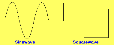
Fig 1: A Sinewave and Squarewave
We are only concerned with the shape of the wave. 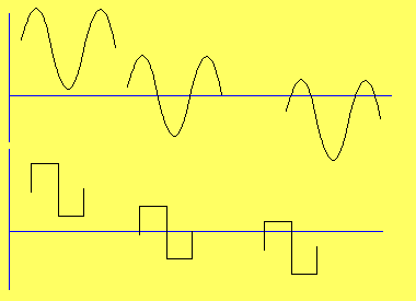
Fig 2: A wave can be anywhere on the axis. It's only
the shape of the wave, we are discussing.
This amazing fact has never been emphasized before. A single resistor or
capacitor has no effect on a waveform.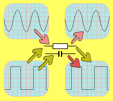
Fig 3: A waveform entering and emerging from a resistor
or capacitor is unaltered!
If two resistors are placed in series, the arrangement is called a Voltage
Divider, Buffer, or Attenuator.
The signal appearing at the join of these two components is equal
to the ratio of the resistances.
The two resistor symbols in Fig 4 have been shown as large and small to make the
description easy to follow.
The signal at the 0v rail will be zero (this is obvious) and as the "tap-off" point is
raised towards the input, the amplitude of the signal will increase, until it is 100% at the top
of the two resistors. The frequency is not affected - only the amplitude
changes.
Both the input and output signals will be IN PHASE. In other words they will both rise and fall at
the same time.
This type of circuit is used to reduce the amplitude of a signal. This is
shown in Fig 4. 
Fig 4: The waveform from a "voltage divider." 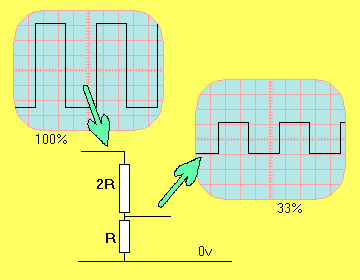
Fig 5: The waveform is attenuated.
Note the position of the small and large capacitor to create signal
attenuation. If you compare this circuit with Fig 5 above, you will notice the
large and small values are in different positions. This is important to remember. 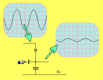
Fig 6: Waveform attenuation using capacitors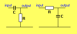
Fig 7: Two ways to connect R and C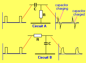
Fig 8: These circuit will be named in a moment.
The capacitor is actually CHARGING during the FALLING part of the graph. And it
is fully charged when the output of the circuit is zero.
This is not obvious from looking at the graph - if you don't know what to look
for - and that's why you have to be able
to read a graph AND look at the the circuit at the same time.
This is the most important part of this discussion.
Waveforms are not easy to read and not easy to interpret.
This is just the beginning of UNDERSTANDING A WAVEFORM.
The input waveform now falls to zero and the voltage across the capacitor
creates a negative pulse across the resistor. To see how this works, we will
replace the capacitor with a small battery. It is identical to a
small battery with the positive terminal being pushed down to the 0v rail.
The negative terminal will go below the 0v rail as shown in the animation below.
This is how the output gets a negative pulse. 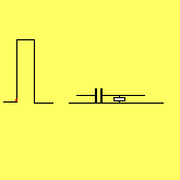
Fig 9: The differentiator in operation
Circuit B creates an entirely different output. The capacitor is designed
to charge fully during the high-time of the pulse and it will then discharge
when the pulse returns to zero.
The current though the resistor is charging the capacitor and when the pulse
returns to zero, the resistor discharges the capacitor.
These two circuits have technical names, they are DIFFERENTIATOR and
INTEGRATOR.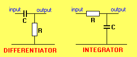
Fig 10: A differentiator and Integrator
This is important as many circuits are not designed as differentiators but
create a negative voltage due to the arrangement of the capacitor and resistor.
This type of circuit is very important as it used in many circuits to connect
one stage to the next.
The following diagram shows a capacitor with an input and output signal.
This type of arrangement is often used to couple two stages and is called "inter-stage coupling." 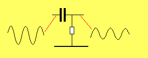
Fig 11: The output follows the input
The following circuit shows capacitor coupling:
Fig 12: Each stage is capacitor coupled
In theory, the waveform on one side of a capacitor will be the same as the other
when a sinewave is applied.
In practice, the shape of the output will depend on the impedance of the circuit
it is connected to.
Let's take the case of a sinewave generator and look at the waveform on both
side of a "coupling capacitor:"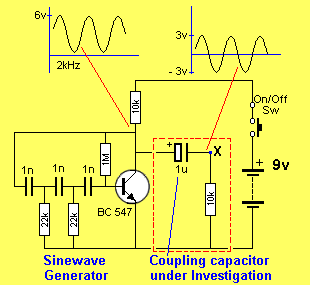
Fig 13: The waveform at point "X"
If the 10k resistor in our circuit under investigation is connected to the 9v rail, the
waveform peaks at 12v and dips to 6v.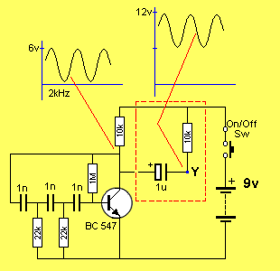
Fig 14: The waveform at point "Y"
The purpose of a coupling capacitor is to separate DC voltages between two stages and transfer
the signal from one stage to the next.
The waveform on the output of the capacitor in Figs 13 and 14 has been delivered
to a high impedance load.
In other words it is not delivering any energy to the load and the waveform will
not attenuated.
But in a normal circuit the capacitor will be delivering energy (commonly
called "a signal") to the stage that follows and this will reduce the amplitude of
the signal.
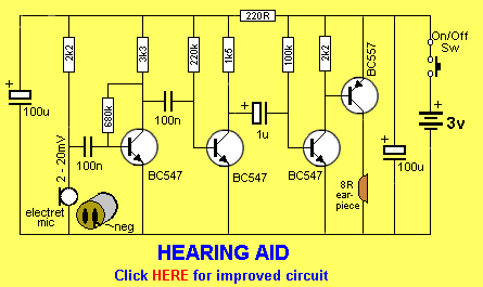
Fig 15: Typical capacitor-coupled stages
If we take the case of a typical capacitor-coupled
amplifier shown in Fig 15, we see the first transistor is "self-biased" and
transistors 2 and 3 are "heavily turned-on."
Now we will see what to expect from this type of biasing:
BIASING A TRANSISTOR
Basically there are three ways to bias a transistor:
1. TOO MUCH
2. TOO LITTLE
3. JUST RIGHT
There are many reasons why a (transistor) stage is not operating correctly. It may be
incorrect biasing, transistor damage, high or low ambient temperature affecting
the bias-point, incorrect
supply voltage or any of a number of other factors.
If a transistor is biased just right it will process a
signal correctly.
If a transistor in an arrangement shown in Fig 16 is not biased correctly, the collector voltage will be too high
or too low and the positive or negative parts of a signal will not be amplified
correctly.
Biasing a transistor has been covered in our
Basic Electronics
Course and you can read more about this in the pay section of
Talking Electronics website.
In general, a transistor must be "turned-on" so that it can amplify both the
positive and negative parts of a signal.
For a simple "self-biased" stage, the collector voltage should be approximately
half-rail voltage, as shown in Fig 16(b).
If the voltage is below half-rail, as shown in Fig 16(b), the transistor is
turned on too much.
If the voltage is above half-rail, as shown in Fig 16(c), the transistor is not
turned enough.
The following diagram shows three biasing arrangements:
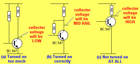
Fig 16: Biasing a transistor
A stage can have faulty biasing due to the gain of the transistor. If a self-bias arrangement is designed for a transistor with medium gain, and a low or high gain device is fitted, the bias-point will change. This is shown in Fig 17, below:
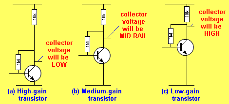
Fig 17: Bias-point depends on the gain of a transistor
The correct biasing of a stage is very important. You must know if a transistor is biased correctly BEFORE taking CRO readings. If the waveform is distorted you need to know if the cause is a faulty component or a biasing problem.
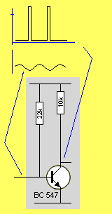
Fig 18: Transistor "saturated" - turned-on too much.
For the transistor in Fig 18 above, the 22k base resistor is
a low value and will turn the transistor ON fully.
The positive excursion of the waveform from the capacitor will not be able to
turn the transistor ON any more, and thus these portions of the signal will not
be processed.
The output will be distorted, as shown in the waveform above.
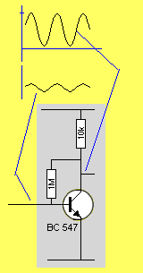
Fig 19: Transistor biased correctly.
The transistor in Fig 19 above is "self biased" via the 1M base resistor and the collector voltage will be approximately mid-rail. This will allow the transistor to process both the positive and negative excursions of the waveform on the base.
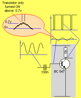
Fig 20: Transistor only turned ON when base
above 0.7v
The transistor in Fig 20 above is not biased via a base resistor.
The positive excursion of the waveform will not be processed until they are
above 0.7v and the negative portions will not be processed AT ALL.
The output will be distorted, as shown in the waveform.
Since 0.7v represents only a very small portion of the amplitude of some
waveforms, it may not be considered as creating distortion.
The arrangement is Fig 20 is a commonly-used configuration called "Class C" in
which the transistor is not biased at all but is turned on via the input signal.
This arrangement has the advantage of drawing zero current when no signal is
being processed and will deliver a large output power.
NEXT
When viewing the waveform on the output of a transistor stage, you need to find
out where the fault is coming from. This will be covered in the next section.
10-03-04